
Introduction
Camera sensitivity is one of the most important aspects of camera performance – with inadequate sensitivity, your imaging experiment may simply be impossible. However, sensitivity is a broad topic dependant on a large number of factors, and cannot be represented by one value alone – while one camera may outperform another at one light level or the exposure time, the situation may be reversed at higher light or longer exposures. This makes it important to understand the main factors behind camera sensitivity in order to best quantify and compare different camera technologies.
Achieving the best sensitivity from a scientific camera is reliant on two main factors:
- Maximizing signal collection
- Minimizing the effect of noise
The relationship between signal and noise is vital for sensitivity and is represented by the signal-to-noise ratio (SNR). In order to perform quantitative imaging it is vital to have a sufficiently high SNR, otherwise signal from your sample can simply be lost in the noise.
For this reason, our scientific cameras are designed to maximize signal collection and minimize noise, as outlined in the rest of the article.
Maximizing Signal Collection
The camera collects signal in photons from the sample in order to generate an image (see previous article). Throughout the signal collection process, the two main factors that affect sensitivity are quantum efficiency and the sensor pixel size.
Quantum Efficiency
Quantum efficiency (QE) is a way to measure how effective a camera sensor is at converting photons into electrons. If a sensor had a QE of 50% and was exposed to 100 photons, it would produce a signal of 50 electrons. This means that the remaining 50% of the photons were never converted and were lost, this really limits the sensitivity of a scientific camera as half of the incident signal was not processed by the camera.
While sensors may not be 100% efficient in practice, QE changes based on several different variables, such as the wavelength of light and the camera technology used. This is outlined in Figure 1.
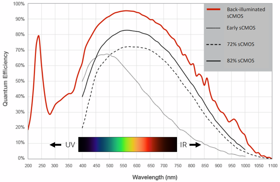
As camera sensor technologies have progressed, QE has increased across all visible light wavelengths, as shown from the insert in Fig.1, as well as increased QE in UV and near-infrared (NIR) regions. Moving to back-illuminated technologies allowed camera sensors to receive more light from samples to the point where imaging with green fluorescence (~550 nm) has a near-perfect QE of 95%, resulting in the highest sensitivities.
By using a camera with high QE across a wide range of wavelengths, and by imaging at peak QE wavelengths, signal collection can be increased. With many life science researchers using blue, green, and red fluorescence, cameras for fluorescence imaging are typically most sensitive across these wavelengths.
Sensor Pixel Size
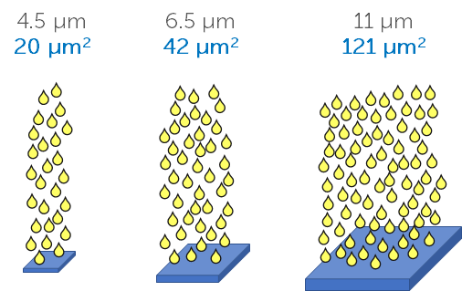
The larger the sensor pixel, the more light it can collect. In order to compare a 4.5 µm pixel with an 11 µm pixel, it is vital to look at the pixel area. The 4.5 x 4.5 pixel has an area of ~20 µm2, while the 11 x 11 pixel has an area of 121 µm2, which is six times the area, this means the 11 µm pixel can collect six times as much signal and is far more sensitive. This is outlined in Figure 2.
Having larger pixels increases the camera sensitivity but typically results in less pixels (as there is a fixed amount of space for a camera sensor, see our field of view note), which reduces the resolution. There is typically a balance between sensitivity and resolution with camera sensors, where the desired characteristic should be prioritised.
Binning
Binning is a setting that exists in most scientific cameras and allows multiple pixels to be combined together in a ‘bin‘. For example, a 2×2 bin combines a 2×2 square of pixels into one single pixel, which would be 4x the area and therefore more sensitive than before. This means that cameras with small pixels to have the option of binning in order to image with larger pixels and increase the sensitivity, at the cost of resolution.
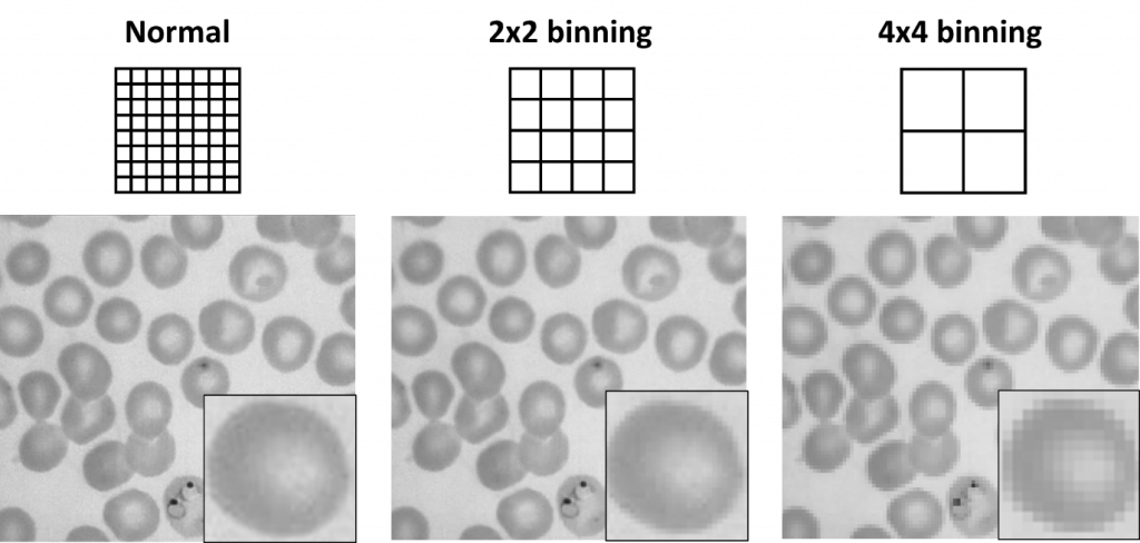
With a CCD/EMCCD the binning occurs before readout and digitization, meaning that both speed (less pixels to process) and sensitivity (larger pixels) will be increased, resulting in a 2×2 bin increasing the SNR by a factor of 4:1. With a CMOS, due to the different sensor format binning occurs off the sensor (or off-chip) and is after the readout, meaning that read noise has already been introduced. This means a 2×2 bin has 4x the signal but 2x the noise, resulting in a SNR increase of 2:1, and no increase in speed. So if imaging with a CMOS, binning will still increase sensitivity, but binning is more effective with CCD/EMCCD cameras.
Minimizing Noise
Noise is error that exists in every measurement made by every camera. When performing imaging experiments, noise is an unavoidable and ever-present factor that needs to be considered, and when possible, minimized. While noise cannot be entirely eliminated, the effects of different kinds of noise can be decreased to the point where they are negligible.
Noise can largely be separated into sample-related noise and camera-related noise, as outlined below.
Sample-related noise
Background fluorescence and other factors can reduce the image contrast depending on how the sample is prepared (e.g. sufficient washing steps after antibody staining, level of room light, etc.), but this is not directly related to noise in the image, more the quality of the signal in the image. Sample-related noise is mostly to do with the way photons travel from the light source (emitted) to the sample, and back to the camera as fluorescence (excited), this is known as photon shot noise.
Photon Shot Noise
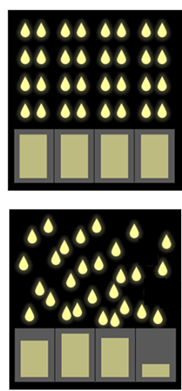
The number of photons produced by a light source (and by the fluorescent probes used in imaging) is not the same each second, and consequently, the number of photons detected by the camera is also not the same each second. Rather than arriving in neatly regimented rows (see Fig.4 top), photons arrive at the sensor like rainfall (see Fig.4 bottom), resulting in uncertainty, which is known as photon shot noise.
This inherent natural source of noise has a square root relationship between the signal and the noise, where a signal of N results in photon shot noise of √N. Shot noise cannot be improved by advances in camera design as it is a physical phenomenon and related to the sample and light source.
Photon shot noise can be lessened with denoising algorithms, used before or during acquisition. One example is the algorithm used by the Prime series of cameras, called PrimeEnhance, and detailed in a separate article.
Camera-Related Noise
Whether using a CCD, EMCCD, or sCMOS camera for scientific imaging, all are subject to certain sources of noise depending on their electronic sensor design. How the sensor deals with photons/electrons, how the sensors are cooled, and any visible patterns/artifacts can all impact camera sensitivity. The main sources of camera-related noise are read noise, dark current noise, and patterns/artifacts.
Read Noise
A camera sensor converts photons into electrons, and then moves these electrons around the sensor to the analog-to-digital converters (ADCs), where the analog electron signal is read and becomes a digital signal. This conversion of analog to digital signals had a fixed value of error, called the read noise. For example, the Prime BSI has a read noise of ±1e–, meaning that a signal of 100 electrons could be read anywhere from 99-101 electrons.
Read noise is different for every sensor, and even between different modes on the same sensor. In order to image at higher speeds, cameras can move electrons around faster and readout faster, but this increases the read noise. In general, read noise is determined by the quality of electronic design and the speed of readout, and has a fixed value for each camera mode.
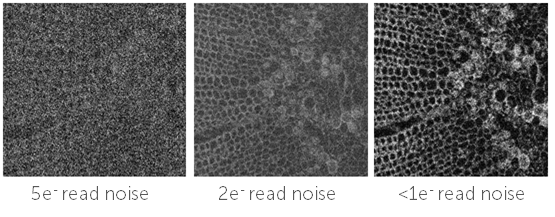
Read noise is most important during high-speed or low-light imaging when signal levels are typically low. If a camera has a read noise of ±2e–. this has a much greater impact on a signal of 10e– than 1000e–. This is why many low-light and low-signal applications are known as read-noise limited, as the main source of noise affecting the images at these levels is the read noise.
CCD cameras typically have a higher read noise from 5-10e–, EMCCDs have a very high base read noise of 80-100e– but use signal multiplication to decrease the effects of read noise, and sCMOS cameras typically have a very low base read noise (1-3e–) as they feature parallel electronic design. By using cameras with elegant and intelligent electronic sensor design, researchers can perform sensitive imaging with ease due to low levels of read noise.
Dark Current Noise
As a camera sensor is exposed to light in order to acquire an image, it can cause the sensor to heat up. This accumulation of thermal energy causes charge to build up on the sensor in the form of thermal electrons, as opposed to the usual photoelectrons generated from photons. Unfortunately, the camera sensor doesn’t know the difference between these types of electrons, and thermal electrons are counted as signal and contribute to noise. This is known as dark current noise.
Dark current is a thermal effect independent from the light level, and can be measured in electrons per pixel per second (e/p/s). Typically, dark current is counteracted with cooling: either forced air cooling (the majority of scientific cameras have a fan) or liquid cooling. For every 6-7°C of cooling, the dark current is halved.
The dark current noise is dependent on the exposure time (the ‘second’ part in e/p/s). The typical dark current of a Photometrics Prime BSI sCMOS is 0.5 e/p/s, meaning that a 2 second exposure would result in 1 electron of dark current per pixel. The important part to consider here is: How long are your exposure times? Typical fluorescence imaging, low-light imaging, and high-speed imaging all feature low signals and short exposure times, well below a second and often below 100 ms. When using a highly-sensitive camera, sufficient signal can be collected in short exposures, and the dark current buildup is negligible.
With modern camera technologies, aggressive and excessive cooling is unnecessary due to the short exposure times. This is why Photometrics cameras such as the Prime BSI Express (no liquid cooling) and the Moment sCMOS (uncooled) can afford to move away from cooling due to their high sensitivity and low exposures, and not experience issues with dark current noise unless exposures of 2 seconds or longer are used.
Patterns/Artifacts
Camera specification sheets and information brochures typically mention the levels of read noise and dark current, but some forms of noise are absent from these spec sheets, such as patterns and artifacts. Variation across a sensor can lead to errors in images, especially when frames are averaged or taken as stacks.
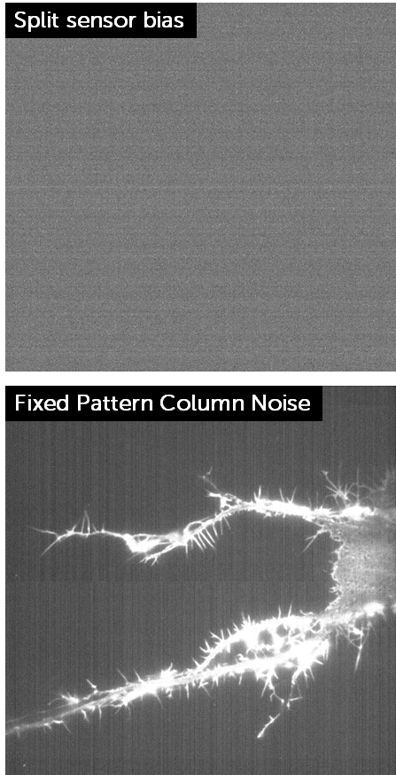
When a camera has very low or no light, the sensor bias can be seen, showing any patterns or artifacts that exist on the sensor. If these patterns exist, they also appear in images as pixel variations. Pattern noise typically appears as a noticeable pattern of ‘hot’ (bright) and ‘cold’ (dark) pixels in the background of images and is produced regardless of the light level.
A classic example is from older front-illuminated sCMOS cameras, which used a split sensor in order to increase the imaging speed, but this split meant that the two sensor halves were not exactly the same, leading to a visible split and the formation of patterns and artifacts, as seen in Fig.5. The patterns are clear both on the camera bias (top of Fig.5, this bias sits in the foundation of every image taken with the camera) and on an average of 100 images (bottom of Fig.5, the patterning here is affecting the signal). This pattern noise can interfere with signal in low-light conditions, reducing the sensitivity of the camera.
Improving Your Signal-To-Noise Ratio
By maximizing signal collection and minimizing noise, we end up with a high signal-to-noise ratio (SNR) and can perform quantitative imaging with high sensitivity. But if signals are low (a common issue in fluorescence imaging), exposures are short or noise is present, it is important to know about your options to increase the SNR, and the trade-offs present.
Increase Exposure Time
Increasing the exposure/integration time allows the camera to collect signal for longer and reach a higher signal level, potentially lifting the signal above the noise floor. However, this would sacrifice the ability to image at a higher frame rate, as speed is often tied to the exposure time (you can only go at 2 frames per second if exposing each frame for 500 ms). Increasing exposure also exposes cells to more light, worsening the effects of phototoxicity and photobleaching if live samples are being used. If the exposure time is long enough, the noise from dark current may also start to become a larger portion of the signal, particularly if exposures go beyond 2-3 seconds.
Increase Light Intensity
Increasing the excitation intensity allows for a higher signal level without having to sacrifice speed as the exposure time is unchanged, but the rate at which phototoxicity occurs is also increased, reducing live cell viability. Even in fixed samples, increased intensity can result in faster bleaching and a reduction of the fluorescent signal.
Frame Averaging
As noise is based on uncertainty, taking a large number of frames and averaging them can decrease the effect of noise, specifically reducing the total noise by the square root of the number of frames averaged. However, this method also sacrifices speed and is generally less effective than increasing exposure time, but keeps the same exposure time in case samples are photosensitive.
Denoising Algorithms
Denoising algorithms increase SNR by reducing the effects of photon shot noise at low light levels, improving the quality of images and data. However, there are many challenges when processing data in this way, such as preserving the recorded pixel intensities and preserving key features like edges, textures, and details with low contrast. Further, processing has to be accomplished without introducing new image artifacts, as some algorithms are inflexible with different image types, resulting in intrusive artifacts. In addition, because noise tends to vary with the signal level, it is difficult for some denoising algorithms to distinguish signal from noise, with small details occasionally being removed. There are many things to consider when denoising, but finding the right algorithm can have big benefits, with some algorithms able to run live on the camera with acquisition.
Improved Camera Specifications
No matter which additional techniques are used for increasing the SNR, using a scientific camera with high sensitivity and low noise characteristics will always be a benefit. A back-illuminated device with 95% quantum efficiency will collect as many incoming photons as possible, combined with a low read noise floor and dark current, this device allows for the detection of the lowest signal levels. Modern scientific cameras also have additional factors such as background quality, field uniformity, and hot-pixel correction – all of which contribute to the scientific camera being a highly sensitive quantitative measurement device.
Summary
Sensitivity is one of the most important aspects of scientific imaging, as with insufficient sensitivity it can be impossible to even find your sample. By maximizing signal collection and minimizing noise levels, sensitivity can be increased to the point where you can perform highly accurate quantitative imaging. Knowledge of the different noise sources and which scientific camera technologies can deliver the highest sensitivities will be a great benefit to your imaging work.