
Introduction
Quantitative scientific cameras are vital for sensitive, fast imaging of a variety of samples for a variety of applications. Camera technologies have advanced over time, from the earliest cameras to truly modern camera technologies, which can push the envelope of what is possible in scientific imaging and allow us to see the previously unseen.
The heart of the camera is the sensor, and the steps involved in generating an image from photons to electrons to grey levels. For information on how an image is made, see our article of the same name. This article discusses the different camera sensor types and their specifications, including:
- Charge-coupled device (CCD)
- Electron-multiplying charge-coupled device (EMCCD)
- Complementary metal-oxide-semiconductor (CMOS)
- Back-illuminated CMOS
This order also shows the chronological order of the introduction of these sensor types, we will go through these one at a time, in a journey through the history of scientific imaging.
Sensor Fundamentals
The first step for a sensor is the conversion of photons of light into electrons (known as photoelectrons). The efficiency of this conversion is known as the quantum efficiency (QE) and is shown as a percentage.
All the sensor types discussed here operate based on the fact that all electrons have a negative charge (the electron symbol being e–). This means that electrons can be attracted using a positive voltage, granting the ability to move electrons around a sensor by applying a voltage to certain areas of the sensor, as seen in Figure 1.
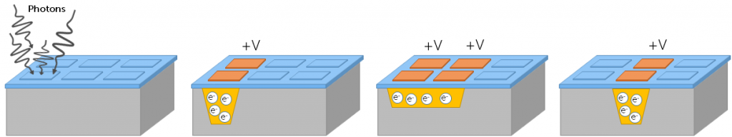
In this manner, electrons can be moved anywhere on a sensor, and are typically moved to an area where they can be amplified and converted into a digital signal, in order to be displayed as an image. However, this process occurs differently in each type of camera sensor.
CCD
CCDs were the first digital cameras, being available since the 1970s for scientific imaging. CCD have enjoyed active use for a number of decades and were well suited to high-light applications such as cell documentation or imaging fixed samples. However, this technology was lacking in terms of sensitivity and speed, limiting the available samples that could be imaged at acceptable levels.
CCD Fundamentals
In a CCD, after exposure to light and conversion of photons to photoelectrons, the electrons are moved down the sensor row by row until they reach an area that isn’t exposed to light, the readout register. Once moved into the readout register, photoelectrons are moved off one by one into the output node. In this node they are amplified into a readable voltage, converted into a digital grey level using the analogue to digital converter (ADC) and sent to the computer via the imaging software.
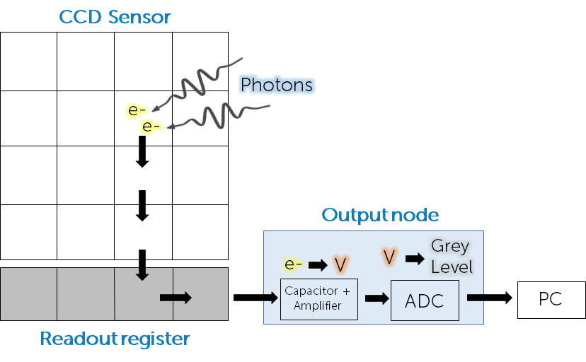
The number of electrons is linearly proportional to the number of photons, allowing the camera to be quantitative. The design seen in Fig.2 is known as a full-frame CCD sensor, but there are other designs known as frame-transfer CCD and interline-transfer CCD that are shown in Fig.3.
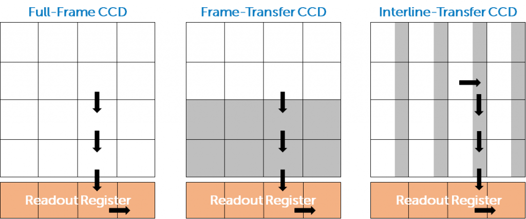
In a frame-transfer CCD the sensor is divided into two: the image array (where light from the sample hits the sensor) and the storage array (where signal is temporarily stored before readout). The storage array is not exposed to light, so when electrons are moved to this array, a second image can be exposed on the image array while the first image is processed from the storage array. The advantage is that a frame-transfer sensor can operate at greater speeds than a full-frame sensor, but the sensor design is more complex and requires a larger sensor (to accommodate the storage array), or the sensor is smaller as a portion is made into a storage array.
For the interline-transfer CCD, a portion of each pixel is masked and not exposed to light. Upon exposure, the electron signal is shifted into this masked portion, and then sent to the readout register as normal. Similarly to the frame-transfer sensor, this helps increase the speed, as the exposed area can generate a new image while the original image is processed. However, each pixel in this sensor is smaller (as a portion is masked), and this decreases the sensitivity as fewer photons can be detected by smaller pixels. These sensors often come paired with microlenses to better direct light and improve the QE.
CCD Limitations
The main issues with CCDs are their lack of speed and sensitivity, making it a challenge to perform low-light imaging or to capture dynamic moving samples.
The lack of speed is due to several factors:
- There is only one output node per sensor. This means that millions of pixels of signal have to be shuttled through one node, creating a bottleneck and slowing the camera.
- If electrons are moved too quickly, it introduces error and read noise, so most CCDs elect to move electrons slower than maximum speed to attempt to reduce noise.
- The whole sensor needs to be cleared of the electron signal before the next frame can be exposed
Essentially, there are very few data readout channels for a CCD, meaning the data processing is slowed. Most CCDs operate at between 1-20 frames per second, as a CCD is a serial device and can only read the electron charge packets one at a time. Imagine a bucket brigade, where electrons can only be passed from area to area one at a time, or a theatre with only one exit but several million seats.
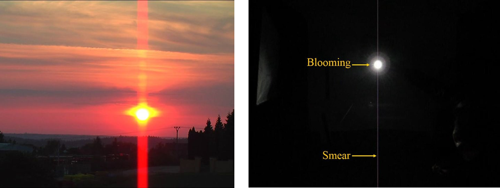
In addition, CCDs have a small full-well capacity, meaning that the number of electrons that can be stored in each pixel is limited. If a pixel can only store 200 electrons, receiving a signal of >200 electrons leads to saturation, where a pixel becomes full and displayed the brightest signal, and blooming, where the pixel overflows and the excess signal is smeared down the sensor as the electrons are moved to the readout register.
In extreme cases (such as daylight illumination of a scientific camera), there is a charge overload in the output node, causing the output amplification chain to collapse, resulting in a zero (completely dark) image.
CCD pixels are also typically quite small (such as ~4 µm) meaning that while these sensors can achieve a high resolution, they lack sensitivity, as a larger pixel can collect more photons. This limits signal collection and is compounded by the limited QE of front-illuminated CCDs, which often only reaches 75% at maximum.
Finally, CCD sensors are typically quite small, with an 11-16 mm diagonal, which limits the field of view that can be displayed on the camera and means that not all of the information from the microscope can be captured by the camera.
Overall, while CCDs were the first digital cameras, for scientific imaging purposes in the modern day they are lacking in speed, sensitivity and field of view.
EMCCD
EMCCDs first emerged onto the scientific imaging scene in 2000 with the Cascade 650 from Photometrics. EMCCDs offered faster and more sensitive imaging then CCDs, useful for low-light imaging or even photon counting.
EMCCDs achieved this in a number of ways. The cameras are back-illuminated (increasing the QE to ~90%) and have very large pixels (16-24 µm), both of which greatly increase the sensitivity. The most significant addition, however, is the EM in EMCCD: electron multiplication.
EMCCD Fundamentals
EMCCDs work in a very similar way to frame-transfer CCDs, where electrons move from the image array to the masked array, then onto the readout register. At this point the main difference emerges: the EM Gain register. EMCCDs use a process called impact ionisation to force extra electrons out of the silicon sensor, therefore multiplying the signal. This EM process occurs step-by-step, meaning users can choose a value between 1-1000 and have their signal be multiplied that many times in the EM Gain register. If an EMCCD detects a signal of 5 electrons and has an EM Gain set to 200, the final signal that goes into the output node will be 1000 electrons. This allows EMCCDs to detect extremely small signals, as they can be multiplied up above the noise floor as many times as a user desires.

This combination of large pixels, back-illumination and electron multiplication makes EMCCDs extremely sensitive, far more so than CCDs.
EMCCDs are also faster than CCDs. In CCDs, electrons are moved around the sensor at speeds well below the maximum possible speed, because the faster the electrons are shuttled about, the greater the read noise. Read noise is a fixed +/- value on every signal, if a CCD has a read noise of ±5 electrons and detects a signal of 10 electrons, it could be read out at anywhere between 5-15 electrons depending on the read noise. This has a big impact on sensitivity and speed, as CCDs move electrons slower in order to reduce read noise. However, with an EMCCD you can just multiply your signal up until the read noise has a negligible effect. This means that EMCCDs can move signal around at maximum speed, resulting in huge read noise values from 60-80 electrons, but signals are often multiplied by hundreds of times, meaning that the read noise impact is lessened. In this manner, EMCCDs can operate at much higher speeds than CCDs, achieving around 30-100 fps across the full-frame. This is only possible due to the EM Gain aspect of EMCCDs.
EMCCD Limitations
Despite the advantages of electron multiplication, it introduces a lot of complexity to the camera and leads to several major downsides. The main technological issues are EM Gain Decay, EM Gain Stability and Excess Noise Factor.
EM gain decay or ageing is a phenomenon that is not fully understood, but essentially involves charge building up in the silicon sensor between the EM electrode and photodetector. This build-up of charge reduces the effect of EM gain, hence EM gain decay. The greater the initial signal intensity and the higher the EM gain, the faster the EM gain will decay. Using an EM gain of 1000x on a large signal would quickly result in EM gain decay. This results in the EM gain not being the same each time, leading to a lack of reproducibility in experiments, limiting the usefulness of the camera as a quantitative imaging tool. EMCCDs essentially have limited lifespans and require regular calibration, leading to these cameras needing to be used in a certain way, limiting the EM gain that can be used in an experiment without damaging the camera. When a camera has been purchased and will be used daily in a research lab, it can be disappointing to learn that the camera will become less and less reliable over time.
In addition, the EM gain process itself is not stable, different fluctuations can occur. One such example is EM gain being temperature-dependent, in order for EMCCDs to have reliable EM gain they typically operate at temperates from -60 ºC to -80 ºC, meaning they require extensive forced-air or liquid cooling. This all adds to the camera complexity and cost, especially if a liquid cooling rig needs to be installed with the camera.
While an EMCCD can multiply signal far above the reaches of read noise, these cameras are subject to other sources of noise, unique to EMCCDs. The number of photons a camera detects is not the same every second, as photons typically fall like rain rather than arrive at the sensor in regimented rows. This disparity between measurements is called photon shot noise. Photon shot noise and other sources of noise all exist in the signal as soon as it arrives on the sensor, and these noise sources are all multiplied up along with the signal, resulting in the Excess Noise Factor. The combination of random photon arrival and random EM multiplication leads to extra sources of error and noise, with all sources of noise (predominantly photon shot noise) being multiplied by a factor of 1.4x. While an EMCCD may eliminate read noise, it introduces its own sources of noise, impacting the signal-to-noise ratio and the ability of the camera to be sensitive.
Finally, the large pixels of an EMCCD lead to these cameras having a lower resolution than CCDs; EMCCDs have a small field of view due to their small sensors; and even today (20 years later) EMCCDs are still the most expensive format of scientific camera.
While EMCCDs greatly improved on the speed and sensitivity of CCDs, they brought their own issues and continued to limit the amount of information that could be obtained from the microscope.
CMOS
While MOS and CMOS technology has existed since before CCD (~1950’s), only in 2009 did CMOS cameras become quantitative enough to be sufficient for scientific imaging, hence why CMOS cameras for science can be referred to as scientific CMOS or sCMOS.
CMOS technology is different to CCD and EMCCD, the main factor being parallelization, CMOS sensors operate in parallel and allow for much higher speeds.
CMOS Fundamentals
In a CMOS sensor there are miniaturized electronics on every single pixel, namely a capacitor and amplifier. This means that a photon is converted to an electron by the pixel, and then the electron is immediately converted to a readable voltage while still on the pixel. In addition, there is an ADC for every single column, meaning that each ADC has far less data to read out than a CCD/EMCCD ADC, which has to read out the entire sensor. This combination allows CMOS sensors to work in parallel, and process data much faster than CCD/EMCCD technologies. By moving electrons much slower than the potential max speed, CMOS sensors also have a much lower read noise than CCD/EMCCD, allowing them to perform low-light imaging and work with weak fluorescence or live cells.

CMOS sensors have also been adopted by the commercial imaging industry, meaning that nearly every smartphone camera, digital camera, or imaging device uses a CMOS sensor. This makes these sensors easier and cheaper to manufacture, allowing sCMOS cameras to feature large sensors and have much larger fields of view than CCD/EMCCD, to the point where some sCMOS cameras can capture all the information from the microscope.
In addition, CMOS sensors had a large full well capacity, meaning they had a large dynamic range and could simultaneously image dark signals and bright signals, not subject to saturation or blooming like with a CCD.
Early CMOS Limitations
Early sCMOS cameras featured much higher speeds and larger fields of view than CCD/EMCCD, and with a range of pixel sizes, there were CMOS cameras that imaged at very high resolution, especially compared to EMCCD. However, the large pixel and electron multiplication of EMCCDs meant that early sCMOS cameras couldn’t rival EMCCD when it came to sensitivity. When it came to extreme low-light imaging or the need for sensitivity, EMCCD still had the edge.

These early sCMOS sensors were front-illuminated and therefore had a limited QE (70-80%), further impacting their sensitivity.
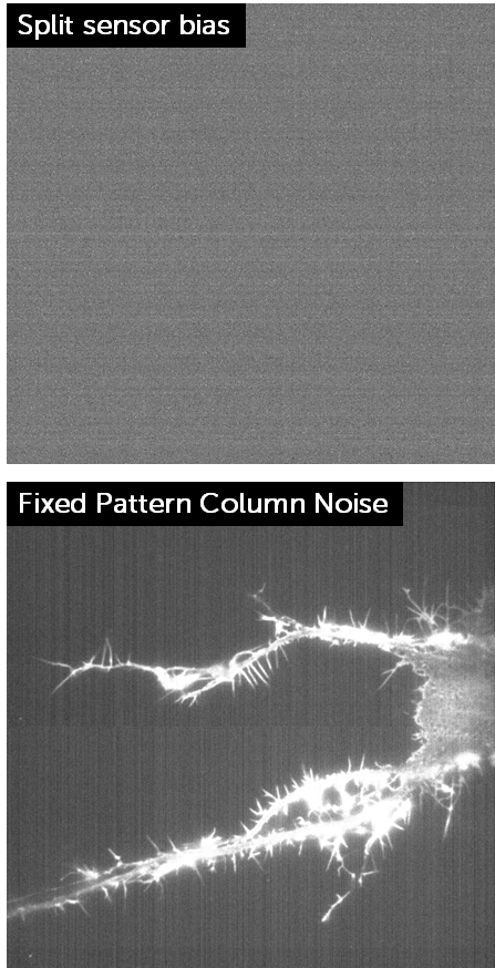
Some early sCMOS, in an effort to run at a higher speed, featured a split sensor, where each half of the sCMOS sensor had its own set of ADCs and the camera image at speeds up to 100 fps. However, this split caused patterns and artifacts in the camera bias, which would be clearly visible in low-light conditions and would interfere with the signal, as seen in Figure 8.
In Fig.8 we can see the bias of a split sensor camera, showing a horizontal line separating the two halves of the sensor, along with the other horizontal scrolling lines. This is due to each sensor half never being exactly the same due to noise and fluctuations. This effect is exacerbated when 100 image frames are averaged, as seen in the lower image. Here the sensor split is also clear, as are vertical columns across the image. This is fixed pattern column noise and is again due to the ADC pairs of the sensor. This noise can interfere with signal in low-light conditions.
This combination of front-illumination, split sensors, patterns/artifacts, and smaller pixels all led to early sCMOS lacking in sensitivity.
Back-Illuminated sCMOS
In 2016 Photometrics released the first back-illuminated sCMOS camera, the Prime 95B. Back-illuminated (BI) sCMOS cameras greatly improve on sensitivity compared to early front-illuminated sCMOS, while retaining all the other CMOS advantages such as high speed, large field of view. The combination of a much higher QE due to back-illuminated (up to 95%, hence the name of the Prime 95B), the single sensor (no split), more varied pixel sizes, and a cleaner background, BI sCMOS is the all-in-one imaging solution.
BI sCMOS Fundamentals
Back-illumination allows for a large increase in camera QE across wavelengths from UV to IR, due to the way that light can access the camera sensor. Figure 9 highlights the differences between a front-illuminated and back-illuminated camera sensor.
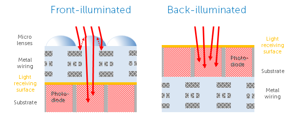
Every stage that light has to travel through will scatter some light, meaning that the QE of front-illuminated cameras is often limited from 50-80%, even with microlenses specifically to focus light onto each pixel. Due to the additional electronics of CMOS sensors (miniaturized capacitor and amplifier on each pixel), there can be even more scattering.
By rotating the sensor and bringing the photodetector silicon layer to the front (from the ‘back’), light has less distance to travel and there is less scattering, resulting in a much higher QE of >95%. While back-illumination was achieved earlier with some CCDs and most EMCCDs, it took longer for CMOS due to the complex electronics involved, and the specific thickness of silicon required to capture different wavelengths of light. Either way, the result is a good 15-20% QE increase at peak, and a 10-15% QE increase out to >1000 nm, doubling the sensitivity in these regions. The lack of microlenses also unlocked a new QE region from 200-400, great for UV imaging.
BI sCMOS have a much greater signal collection ability than FI sCMOS due to the increase in QE and the elimination of patterns/artifacts with a clean background. Along with the low read noise, BI sCMOS is able to match and outperform EMCCD in sensitivity, as well as already featuring much higher speed, resolution, and larger field of view.
Summary
Scientific imaging technologies have continued to advance from CCD, to EMCCD, sCMOS, and back-illuminated sCMOS, in order to deliver the best speed, sensitivity, resolution, and field of view for your sample on your application. Choosing the most suitable camera technology for your imaging system can improve every aspect of your experiments and allow you to be quantitative in your research. While CCD and EMCCD technologies enjoyed popularity in scientific imaging, over the past few decades sCMOS technology has come to the fore as an ideal solution for imaging in life sciences.