
Introduction
There is often a focus on getting a suitable pixel size depending on the experiment, application, or microscopy technique. An easy way to change sensor pixel size is to combine pixels into larger ‘superpixels’, also known as binning, which can affect both the sensitivity and speed of a scientific camera depending on your camera type, whether CCD/EMCCD or CMOS.
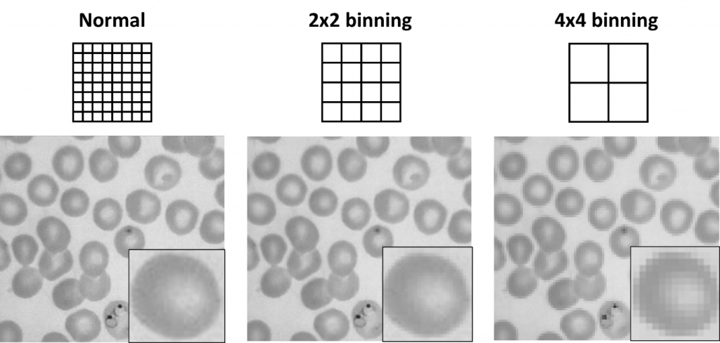
When binning, squares of pixels are ‘binned’ into larger pixels. With a 2×2 bin, a square of 2×2 (4) pixels are read out by the camera as if they were a single pixel. Binning can range from 2×2 up to extremes such as 32×32 depending on the limits imposed by the manufacturer and your camera sensor technology (CCD/EMCCD or CMOS). The effect of no binning, a 2×2 bin, and a 4×4 bin can be observed in Fig.1.
It should be noted that binning differs depending on camera technology, namely charge-coupled device (CCD), electron-multiplied CCD (EMCCD) or complementary metal-oxide-superconductor (CMOS) sensors.
CCD/EMCCD Binning
When a CCD/EMCCD sensor is binned it occurs on the sensor before readout, meaning that it occurs before read noise is introduced by converting photoelectrons (analog voltage signal) into grey levels (digital signal). The two primary benefits of binning with CCD/EMCCD is the improved signal-to-noise ratio (SNR) and the increased frame rate.
The result is that each readout event from the sensor contains the collected charge from all the binned pixels, so four pixels for a 2×2 bin. It should be noted that Teledyne Photometrics cameras have the ability to perform binning into any arbitrary MxN binned pixels (superpixels) through simple software control. Since both the serial register and summing well accumulate charge from multiple pixels during binning, they must have sufficient capacity to prevent saturation. The specifications of the particular CCD/EMCCD being used should be noted and understood before binning. This is especially true when working at high-illumination levels where saturation could lead to erroneous data collection.
The effect of CCD/EMCCD binning improves both the SNR and the speed. The SNR is improved as the read noise is only added to each superpixel. In a 2×2 bin, the signal is improved by four times (as each superpixel is four pixels), meaning the SNR is boosted by a factor of 4:1 (signal:noise). This has a great impact on the ability to image weak signals, as the camera is far more sensitive. However, it should be noted that binning does not lessen the effects of other noise sources, such as dark current noise or photon shot noise.
Binning with CCD/EMCCDs also improves the frame rate (acquisition speed) of the camera, this is due to the slowest step in readout being the digitization of each pixel, and binning reducing the number of effective pixels. Thus, highly binned, low-resolution images can be obtained when high speed is required (such as in focusing) and full-frame, high-resolution images can be obtained when the ultimate resolution is required. Because this can all be controlled via software, Teledyne Photometrics CCD/EMCCDs are extremely flexible and can be used in a wide variety of analytical imaging applications.
CMOS Binning
The sensor format of CMOS cameras is different from CCD/EMCCD sensors, meaning binning also works differently. In CMOS the binning occurs off the sensor, after readout. This means that read noise has already been introduced to each pixel. Combining a 2×2 section of pixels together results in double the read noise for that resulting super‑pixel. Overall, it is four times the signal but two times the read noise, meaning only a 2:1 boost in SNR, compared to 4:1 in CCD/EMCCD. In addition, as it occurs off-chip after readout, there is no speed benefit as the pixels have already been digitized. However, CMOS cameras are far faster than CCD/EMCCD in general, meaning high speeds are still easily achievable.
CMOS Binning: Worked Example
Consider that there are only three major noise sources: photon shot noise, read noise, and dark current.
- Shot noise: If we detect 50 e- of signal, the shot noise is √50 or ~7 e-.
- Read noise: A fixed value for the sensor, for this case it is 1.7 e-
- Dark current: The image is taken with a short exposure (<1 s), so the dark current is effectively 0 e-.
This does not mean the total noise for this image is 8.7 e- (the total of the three noises). When adding noise together you take each value, square it, add the squares and take the square root of the result. This is called ‘adding in quadrature’. Our equation looks more like this:

The noise in this situation is dominated by shot noise, the effect of read noise and dark current is largely negligible. This results in an SNR of ~50:7 or ~7:1. But while the noise is added in quadrature, the signal is added normally. If we perform a 2×2 bin on four pixels that each have the same signal of 50 e- and the same noise values, we have a signal of 200 e- (50+50+50+50), but the noise of:

After a 2×2 bin, this gives us a new SNR of ~200:14 or ~13:1. Compared to the 7:1 before binning, the 13:1 after a 2×2 bin results in double the signal-to-noise ratio, increasing the imaging sensitivity of the camera.
Summary
Binning allows cameras to artificially increase pixel size in order to gather more signal at the cost of resolution, increasing the flexibility of a camera sensor. Due to the manner in which different camera sensors work, it is important to note the differences in binning between CMOS and CCD/EMCCD.