Saturation and Blooming
Saturation and blooming are phenomena that occur in all cameras and it can affect both their quantitative and qualitative imaging characteristics. If each individual pixel can be thought of as a well of electrons, then saturation refers to the condition where the well becomes filled. The amount of charge that can be accumulated in a single pixel is determined largely by its area. However, due to the nature of the potential well, which holds charge within a pixel, there is less probability of trapping an electron within a well that is approaching saturation. Therefore, as a well approaches its limit, the linear relationship between light intensity and signal degrades. As a result, the apparent responsivity of a “saturated” pixel drops.
At saturation, pixels lose their ability to accommodate additional charge. This additional charge will then spread into neighboring pixels, causing them to either report erroneous values or also saturate. This spread of charge to adjacent pixels is known as blooming and appears as a white streak or blob in the image.
In addition, because this extra-large number of electrons needs to be moved down the sensor in order to be read by the CCD readout register, moving this saturated spot causes a vertical streak/smear down the image, further disrupting the image acquisition. Examples of blooming and smearing can be seen in Fig.1.
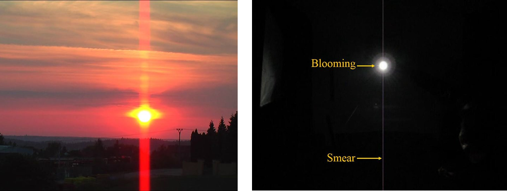
Left Picture of a sunset. The sun is so bright in the image that there is blooming on the sun itself, leaking into the surrounding pixels, and a vertical smear across the whole image.
Right Similar situation with the blooming and smear labeled.
Because various scientific cameras contain different architectures, saturation and blooming can be defined and controlled in many ways.
Linear Full Well
As the well starts to fill, the photometric response of the pixel departs from linearity. The point at which this deviation exceeds an acceptable level is defined as linear full well. Cameras are usually designed so that this signal level fills the full (12-bit, 14-bit, or 16-bit) dynamic range of the analog-to-digital converter.
Noise Clipping
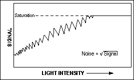
One can see signs of saturation even before the linear full well condition is reached. As the wells fill, the random noise (square root of the signal) starts to be clipped at the top end. As a result, a condition termed “noise clipping” can be observed where the signal noise starts to decrease even though the signal is still increasing.
Output Stage Saturation
When many pixels on a camera are saturated, or when extensive parallel and serial binning is being performed, the output stage may saturate. Under extreme conditions (say, daylight illumination of a scientific camera), the charge overload in the output node can cause the output amplification chain to collapse, resulting in a zero (completely dark) image.
It should be noted that in all cameras, wells can hold more than they can transfer. When they begin to fill, the saturation we observe is actually caused by approaching this maximum charge-transfer condition.
Blooming can be controlled in a couple of ways. For instance, a multiphase CCD can be partially clocked during integration to eliminate image blooming. During integration, two of the three clock-voltage phases used to transfer charge between neighboring pixels are alternately switched. When a pixel approaches saturation, excess charge is forced into the barrier between the Si and SiO2 layers, where it recombines with holes. As the phases are switched, excess charge in pixels approaching saturation is lost, while the charge in non-saturated pixels is preserved. As long as the switching period is fast enough to keep up with overflow signal generation, charge will not spread into neighboring pixels. Known as “clocked anti-blooming”, this technique is most appropriate for low-light applications.
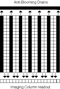
Anti-blooming is traditionally controlled by specific CCD architecture design. Some cameras utilize CCDs that have charge drains running in a strip between every other column. Excessive charge that would normally cause blooming is siphoned off into this drain. Although such an architecture causes a reduction in the effective quantum efficiency and modulation transfer function (MTF), these devices are invaluable when light intensities span many orders of magnitude within a single image.