
Alexander Impertro, Julian Wienand, Prof. Monika Aidelsburger
Quantum Optics Group, Ludwig-Maximillian University of Munich, Germany
Background
Alexander Impertro and Julian Wienand are both PhD students in the group of Prof. Monika Aidelsburger and Prof. Immanuel Bloch at the LMU Munich, working on experiments with ultra-cold atoms for analog quantum simulation.
They took us through the concepts behind their work, “The idea is that by taking very cold atoms and trapping them in lattices generated by interfering laser beams, one can simulate the behavior of electrons in a real solid. The atoms hereby play the role of the electrons and the potential landscape generated by the laser beams mimics the ion crystal. This effectively simulates quantum phenomena in real solids with the benefit that the atoms can be controlled in a targeted way, as typical length scales in the analog quantum simulator are thousands of times larger than in real solids.”
“The quantum simulator is highly tunable. By changing the depth of the lattice and the value of an external magnetic field, the dimensionality of the lattice, the strength of the atom tunneling, or the magnitude of the interactions can all be adjusted, in order to simulate tailored systems and phenomena.”
The Quantum Optics Group requires an imaging setup in order to determine which site of their lattice is occupied with atoms and which site is not. In order to do this, the lattice intensity can be increased to ‘freeze’ the atoms in place, then near-resonant lasers can be used to excite the atoms, these atoms then fluoresce and the scattered photons can be detected with a camera.
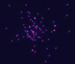
with the Kinetix22 sCMOS.
Challenge
Mr. Impertro and Mr. Wienand described the challenges they face, “Exciting the atoms with our laser heats them up and will cause them to move, so the atoms only fluoresce for around 100 milliseconds to 1 second before they tunnel to another site of the lattice. During that time, we need to acquire an image where we see the single atoms in their lattice sites. In order to get high signal-to-noise ratios, we require high quantum efficiencies and low electronic noise combined with a high frame rate.”
“The better the signal to noise ratio, the shorter we have to image in order to get the same image quality, so what’s important is that the camera has low noise. In order to carefully analyze the quality of the imaging technique, it is also important to take many images of the same atom cloud. Typically, we want to take 10 or more images at exposures of 100 ms each and a small delay between them.”
Another challenge is that the detected wavelength is in the near-infrared (NIR) region of the spectrum, at 852 nm. This means a camera with a broad QE range and good NIR sensitivity is required in order to achieve good signal-to-noise ratios. For high-quality and high-resolution images it is further beneficial to work with small pixel sizes in order to reduce the complexity of the optical setup. Moreover, having a large sensor available significantly simplifies finding a first signal from the atomic cloud, thereby simplifying experimental alignment procedures.
The Kinetix22 is a huge improvement for us, with a great signal to noise ratio, small pixel, and a large chip size.
Solution
The Kinetix22 sCMOS is a flexible and powerful camera with numerous physical science applications, particularly for quantum-based projects. The large 22 mm sensor, fast readout speeds, small pixels, and sub-electron read noise result in an ideal solution for this application.
Mr. Impertro and Mr. Wienand told us about their experience with the Kinetix22, “Previously, we used a camera with much longer readout times, around 800 ms. Compared to this the Kinetix22 is a huge improvement for us as we can take several measurements of the same cloud one after another.”
“We found that the Kinetix22 Sub-Electron mode gave us a great signal-to-noise ratio, so we plan to use this mode in the future for our experiments. What we also like about the Kinetix22 is that the pixel size is small, so we don’t need to work with large magnifications. A previous camera with 13 μm pixel size meant we had to use a magnification of at least 100x, now thanks to the 6.5 μm pixel size of the Kinetix22 we can use 40-60x, which makes our imaging path much shorter.”
“The 22 mm chip size is also much larger than our previous camera and this makes it much easier to find the atoms in the system, which is very useful. We used the USB connector with the Kinetix22, this was really easy plug and play, this was something we liked a lot.”
