
Introduction
The detector is one of the most important components of any microscope system. Accurate detector readings are vital for collecting reliable biological data to process for publication.
To ensure your camera is performing as well as it should be, Photometrics designed a range of tests that can be performed on any microscope. The results of these tests will give you quantifiable information about the state of your current camera as well as providing a method to compare cameras, which may be valuable if you’re in the process of making a decision for a new purchase.
This document will first take you through how to convert the measured signals into the actual number of detected electrons and then use these electron numbers to perform the tests. The tests in this document make use of ImageJ and Micro-Manager software as both are powerful and available free of charge.
Table of Contents
Working With Photoelectrons
- Measuring Photoelectrons
- Measuring Camera Bias
- Calculating Camera Gain
- Calculating Signal to Noise Ratio (SNR)
Testing Camera Quality
- Evaluating Bias Quality
- Evaluating Gain Linearity
- Calculating Read Noise
- Calculating Dark Current
- Counting Hot Pixels
Other Factors To Consider
- Saturation and Blooming
- Speed
- Types of Speed
- Binning and Regions of Interest (ROI)
- Quantum Efficiency
- Pixel Size
- Pixel Size and Resolution
Working With Photoelectrons
Measuring Photoelectrons
A fluorescence signal is detected when photons incident on the detector are converted into electrons. It’s this electron signal that’s converted by the analog-to-digital converter (ADC) in the camera to the Grey Levels (ADUs) reported by the computer. Although grey levels are proportional to signal intensity, not every camera converts electrons to the same number of grey levels which makes grey levels impractical for quantifying signal for publication. Instead, the signal should be quantified in photoelectrons as these are real-world values for intensity measurement that allow for consistent signal representation across all cameras. This signal can then be compared against noise to assess the quality of images by signal to noise.
To convert signal in grey levels to signal in electrons:
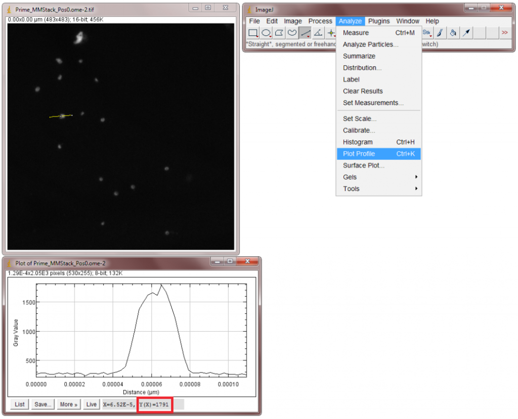
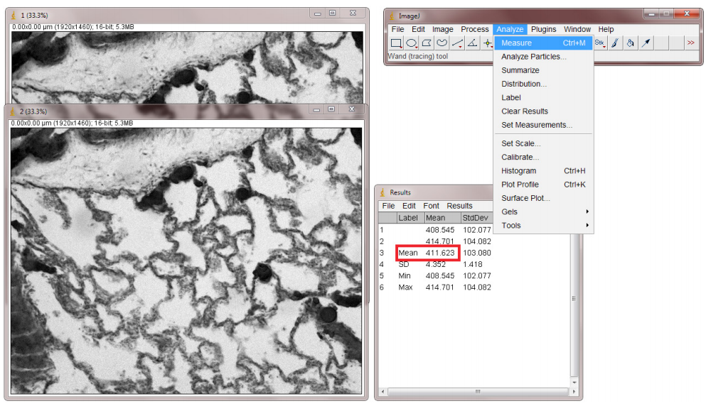
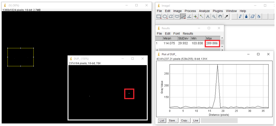
- Load an image into ImageJ, pick a fluorescent spot, and draw a line across it.
- Select Plot Profile from the Analyse menu (Figure 1) to get a peak representing the signal across the line in Grey Levels. Find the value at the top of the peak.
- Subtract the camera bias from this Grey Level signal.
- Multiply the result by the camera system gain.
The full equation is:
Signal in Electrons = Gain x (Signal in Grey Levels – Bias)
The camera bias and camera system gain can be found on the Certificate of Performance (COP) or other information provided with the camera, these values can also be calculated by tests explained below.
As an example, the data in Fig.1 was taken with the Prime 95B™ which has a bias of ~100 and using a gain state of ~1.18. By inserting these values into the equation, we get the following result:
Signal in Electrons = 1.18 x (1791 – 100)
Signal = 1995 e-
Measuring Camera Bias
When visualizing a fluorescence image, we would expect the intensity value of a pixel to correspond only to the intensity of fluorescence in the sample. However, every camera has a background offset that gives every pixel a non-zero value even in the absence of light. We call this the camera bias.
The bias value is necessary to counteract fluctuating read noise values which might otherwise go below zero. The value of the bias therefore should be above zero and equal across all pixels. The bias value doesn’t contain any detected signal so it’s important to subtract it from an image before attempting to calculate the signal in photoelectrons.
To calculate the camera bias:
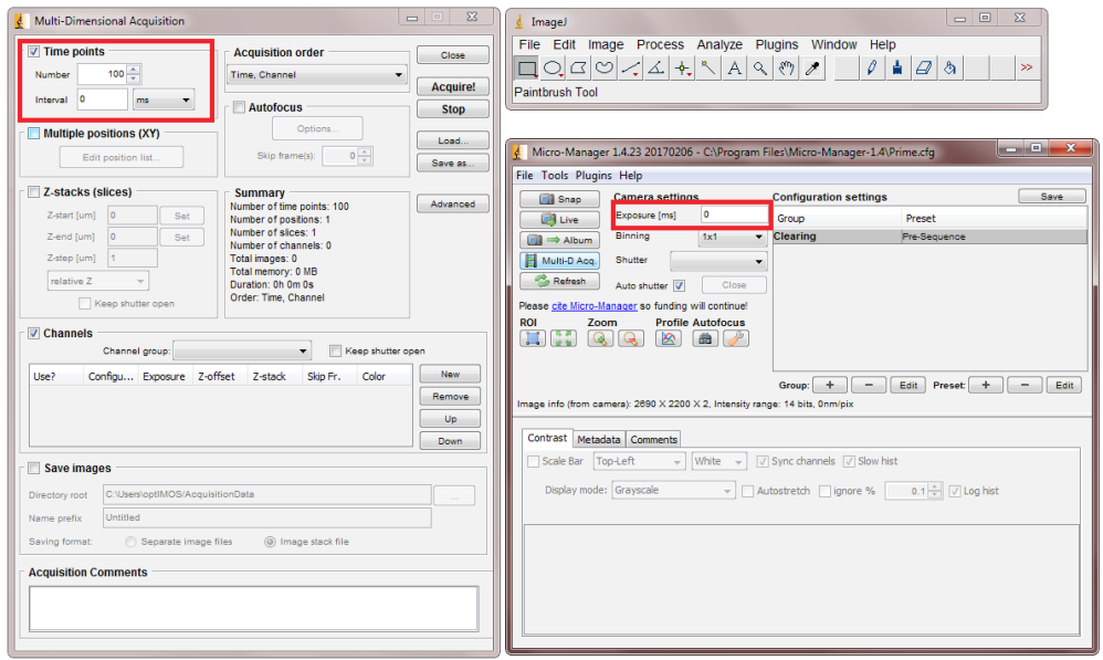
- Set your camera to a zero millisecond exposure time.
- Prevent any light from entering the camera by closing the camera aperture or attaching a lens cap.
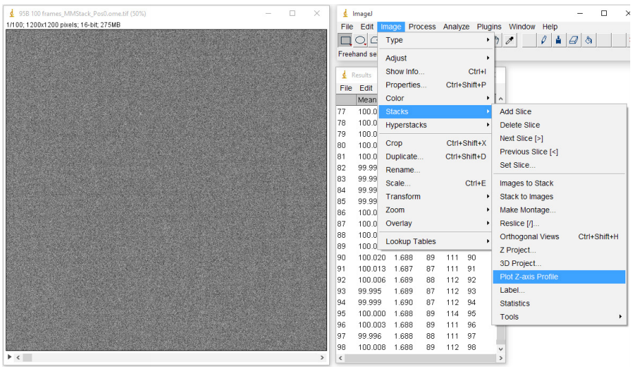
- Take 100 frames with these settings (see Fig.2)
- Calculate the mean of every frame by selecting Stacks from the Image menu and then clicking on Plot Z-axis profile (Fig.3). This should give you the mean values of every frame in the Results window.
- Calculate the mean of the 100 frame means by selecting Summarize in the Results menu.
- The bias is the mean of a single frame, so by plotting the mean values of all 100 frames we calculate a more accurate bias.
Calculating Camera Gain
When the amount of light entering a camera is linearly increased, the response of the camera in grey levels should also linearly increase. The gain represents the quantization process as the light incident on the detector is processed and quantified. It varies from camera to camera depending on electronics and individual properties but it can be calculated experimentally. If a number of measurements are made and plotted against each other the slope of the line should represent the linearity of the gain.
Camera system gain is calculated by a single point mean-variance test which calculates the linear relationship between the light entering the camera and the cameras response to it. To perform this test:
- Take a 100-frame bias stack with your camera (as in the previous section) and calculate the mean bias.
- Take 2 frames of any image using the same light level with a 5 ms exposure time.
- In ImageJ Analyze menu, Measure the means of both images and average them (Fig.4).
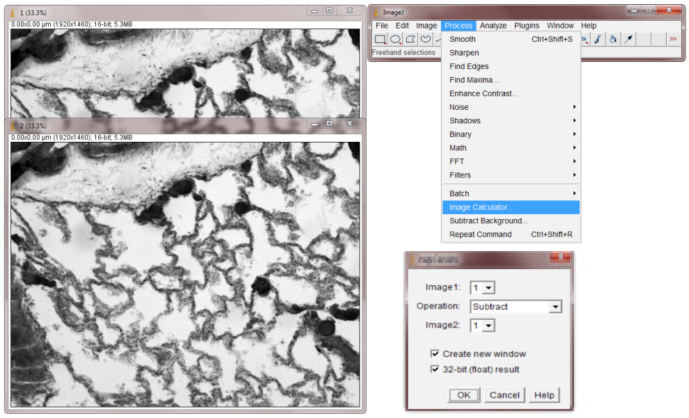
- Calculate the difference between the two images by selecting Image Calculator from the Analyze menu. Select the two frames and Subtract. Press OK to generate a diff image (Fig.5).
- Measure the Standard Deviation of the diff image.
- Calculate the variance of the two images with the following equation: Variance (Image 1, Image 2) = Standard Deviation2 / 2
- Calculate the gain from the variance using the following equation (gain represented as e-/grey level): Gain = (Mean – bias) / Variance
- Repeat this process with 10ms, 20ms, and 40ms exposure times to check that the gain is consistent across varying light levels.
- You can also use the single-point mean-variance (gain) calculator provided by Photometrics.
Calculating Signal to Noise Ratio (SNR)
The SNR describes the relationship between the measured signal and the uncertainty of that signal on a per-pixel basis. It is essentially the ratio of the measured signal to the overall measured noise on a pixel. Most microscopy applications look to maximize signal and minimize noise.
All cameras generate electron noise with the main sources being read noise, photon shot noise, and dark current. These noise values are displayed on the camera datasheet and are always displayed in electrons. This means that the most accurate way to calculate the SNR is by comparing signal in electrons to noise in electrons.
The SNR can be calculated using the following equation:
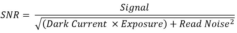
The best way to calculate an electron signal for use in the equation is to use a line profile across an area of high fluorescence.
You can also use the signal to noise calculator provided by Photometrics.
Testing Camera Quality
Evaluating Bias Quality
There are two important things to look for in bias: stability and fixed pattern noise.
Stability is simply a factor of how much the bias deviates from its set value over time. A bias that fluctuates by a large amount will not give reliable intensity values.
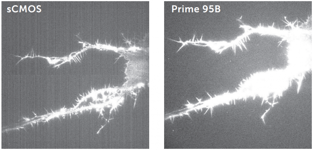
Fixed pattern noise is typically visible in the background with longer exposure times and it occurs when particular pixels give brighter intensities above the background noise. Because it’s always the same pixels, it results in a noticeable pattern seen in the background. This can affect the accurate reporting of pixel intensities but also the aesthetic quality of the image for publication.
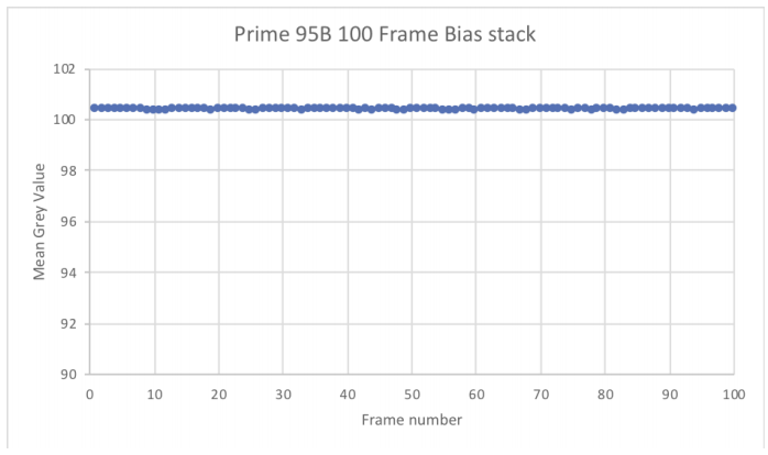
To evaluate the bias stability:
- Plot the mean values of 100 bias frames.
- Fit a straight line and observe the linearity
Our goal at Photometrics is to produce a stable bias that doesn’t deviate by more than one electron, which is shown here using the Prime 95B™ Scientific CMOS data (Fig.6).
To evaluate fixed pattern noise:
- Mount a bright sample on the microscope and illuminate it with a high light level
- Set the exposure time to 100 ms
- Snap an image
- Repeat this experiment with longer exposure times if necessary
A ‘clean’ bias, such as that with the Prime 95B, results in higher quality images and more accurate intensity data, as seen in Fig.7. Fixed pattern noise seen in some split sensor sCMOS cameras can interfere with imaging.
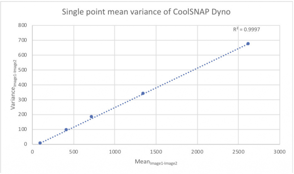
Evaluating Gain Linearity
Gain linearity is very important as the gain directly influences how the electron signal is converted into the digital signal read by the computer. Any deviation from a straight line represents inaccurate digitization.
To evaluate the gain linearity:
- Plot the mean of two images against the variance of two images (such as that collected from Calculating Camera Gain)
- Fit a straight line and observe the linearity
Photometrics recommends that any deviation from the line be no more than 1%, as shown in Fig.8 using data from a CoolSNAP™ DYNO scientific camera.
Calculating Read Noise
Read noise is present in all cameras and will negatively contribute to the signal to noise ratio. It’s caused by the conversation of electrons into the digital value necessary for interpreting the image on a computer. This process is inherently noisy but can be mitigated by the quality of the camera electronics. A good quality camera will add considerably less noise.
Read noise will be stated on the camera datasheet, certificate of performance, or other information provided with the camera. It can also be calculated as explained below.
Read noise can be calculated with the following method:
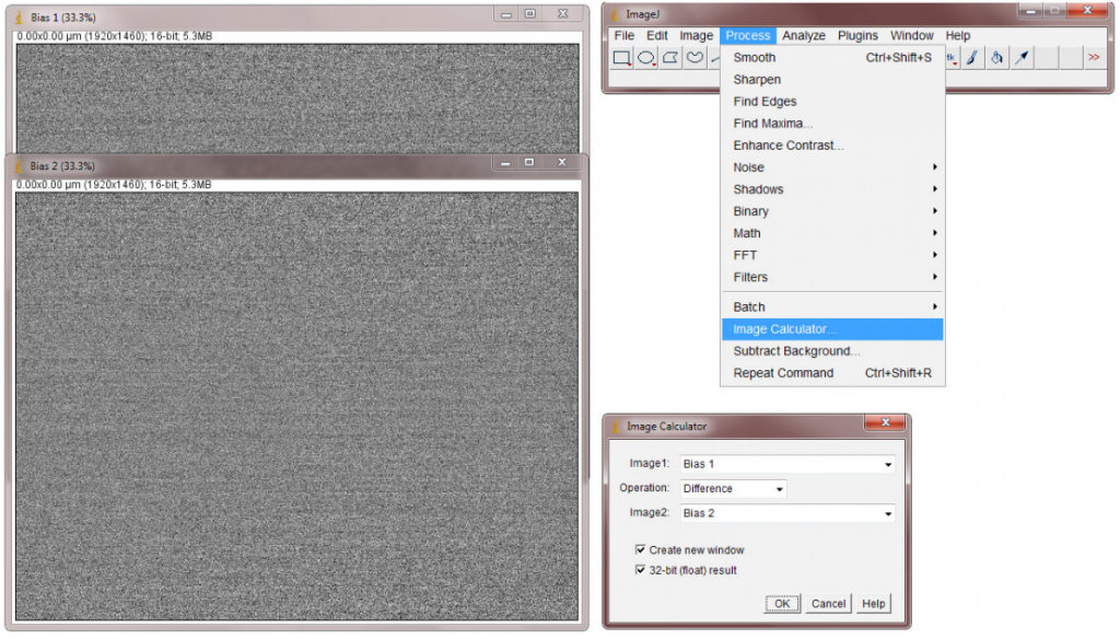
- Take two bias images with your camera
- In ImageJ, calculate the difference between the two images by selecting Image Calculator from the Analyze menu. Select two frames and Subtract, you will need to float the result (32-bit). Press OK to generate the diff image (Fig.9).
- Measure the Standard Deviation of the diff image.
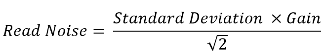
- Use the following equation to calculate system read noise, you’ll need the previously calculated gain value or you can use the gain value given with the camera (in a certificate of performance)
You can also use the read noise calculator provided by Photometrics.
Calculating Dark Current
Dark current is caused by thermally generated electrons which build up on the pixels even when not exposed to light. Given long enough, dark current will accumulate until every pixel is filled. Typically, pixels will be cleared before an acquisition but dark current will still build up until the pixels are cleared again. To solve this issue, the dark current is drastically reduced by cooling the camera. You can calculate how quickly dark current builds up on your camera with the method below.
To calculate how much dark current is accumulating over differing exposure times, you need to create a dark frame. A dark frame is a frame taken in the dark or with the shutter closed. By creating multiple dark frames with varying exposure times or acquisition times, you can allow more or less dark current to build up. To do this:
- Prevent any light from entering the camera and take images at exposure times or acquisition times you’re interested in. For example, you may use a 10 ms exposure time but intend to image for 30 seconds continuously. In this case, you should prepare a 30 second dark frame.
- Take two dark frames per time condition.
- In ImageJ, calculate the difference between the two dark frames by selecting Image Calculator from the Analyze menu. Select the two frames and Difference, you will need to float the result.
- Measure the Standard Deviation of the diff image.
- Use the same equation as the read noise section above to calculate both read noise and dark current. The equation remains the same as in the previous section but because the camera has exposed for a certain amount of time, the dark current has built up on top of the read noise.
- Subtract the number of electrons contributed by read noise (calculated in the previous section), this leaves the noise contributed by dark current.
- Compare the calculated dark current value to the acquisition time to determine how much dark current is built up per unit time.
- Repeat at differing exposure times and temperatures to determine the effect of cooling on dark current build up.
Counting Hot Pixels
Hot pixels are pixels that look brighter than they should. They are caused by electrical charge leaking into the sensor wells which increases the voltage at the well. They are an aspect of dark current so the charge builds up over time but they are unable to be separated from other forms of dark current.
To identify hot pixels:
- Take a bias frame with your camera.
- Prevent any light from entering the camera and take a 10 frame stack with a long (~5 sec) exposure.
- In ImageJ, subtract the bias frame from one of the long exposure frames using the Image Calculator from the Analyze menu.
- Hot pixels should immediately be visible as bright white spots on a dark background, draw line profiles over individual hot pixels to measure intensity (Fig.10).
- Compare hot pixels on all 10 long exposure frames.
Hot pixels always stay in the same place so once they are identified these pixels can be ignored for data processing. Like normal dark current, camera cooling drastically reduces hot pixel counts. If you are still having issues with hot pixels you may be able to adjust the fan speed of the camera to provide more cooling or even switch to a liquid-cooled system.
Other Factors To Consider
Saturation and Blooming
Saturation and blooming occur in all cameras and can affect both their quantitative and qualitative imaging characteristics.
Saturation occurs when pixel wells become filled with electrons. However, as the pixel well approaches saturation there is less probability of capturing an electron within the well. This means that as the well approaches saturation the normally linear relationship between light intensity and signal degrades into a curve. This affects the ability to accurately quantify signal near saturation. To control for saturation, we call the full well capacity before it starts to curve off the linear full well capacity. A high-quality camera will be designed so that the linear full well capacity fills the full 12-, 14- or 16-bit dynamic range so no signal is lost. At Photometrics, we always restrict the full well capacity to the linear full well so you’ll never experience saturation effects.
An additional saturation problem is that when the pixel reaches saturation, the extra charge can spread to neighbouring pixels. This spread is known as blooming and causes the neighbouring pixels to report false signal values. To control for blooming, Photometrics cameras feature the anti-blooming technology, clocked anti-blooming. In this technique, during an exposure, two of the three clock voltage phases used to transfer electrons between neighbouring pixels are alternately switched. This means that when a pixel approaches saturation, excess electrons are forced into the barrier between the Si and SiO2 layers where they recombine with holes. As the phases are switched, excess electrons in pixels approaching saturation are lost, while the electrons in non-saturated pixels are preserved. As long as the switching period is fast enough to keep up with the overflowing signal, electrons will not spread into neighbouring pixels. This technique is very effective for low-light applications.
Speed
Biological processes occur over a wide range of time scales, from dynamic intracellular signalling processes to the growth of large organisms. To determine whether the speed of your camera can meet the needs of your research, you need to know which aspects of the camera govern its speed. These aspects can be broken down to readout speed, readout rate, readout time and how much of the sensor is used for imaging.
Readout speed tells you how fast the camera is able to capture an image in frames per second (fps). For a camera with a readout speed of 100 fps, for example, you know that a single frame can be acquired in 10 ms. All latest model Photometrics cameras are able to show hardware generated timestamps that give much more reliable readout speed information than the timestamps generated by imaging software. This can be shown in PVCAMTest provided with the Photometrics drivers or turned on in MicroManager by enabling metadata. The .tiff header will then show the hardware generated timestamps.
Readout rate tells you how fast the camera can process the image from the pixels. This is particularly important for CCD and EMCCD cameras which have slow readout rates because they convert electrons into a voltage slowly, one at a time, through the same amplifier.
CMOS cameras have amplifiers on every pixel and so are able to convert electrons into a voltage on the pixel itself. This means that all pixels convert electrons to voltage at the same time. This is how CMOS devices are able to achieve far higher speeds than CCD and EMCCD devices, they have far higher readout rates.
Readout rate is typically given in MHz and by calculating 1/readout rate you can find out how much time the camera needs to read a pixel.
Readout time is only relevant for sCMOS devices and tells you the readout rate of the entire pixel array. This can be calculated as 1/readout speed, so if the readout speed of the camera is 100 fps, the readout time is 10 ms.
Binning and Region of Interest (ROI)
When speed is more important than resolution, pixels can be binned or a ROI can be set to capture only a subset of the entire sensor area.
Binning involves grouping the pixels on a sensor to provide a larger imaging area. A 2×2 bin will group pixels into 2×2 squares to produce larger pixels made up of 4 pixels. Likewise, a 4×4 bin will group pixels into 4×4 squares to produce larger pixels made up of 16 pixels, and so on.
On a CCD or EMCCD, binning increases sensitivity by providing a larger area to collect incident photons as well as increasing readout speed by reducing the number of overall pixels that need to be sent through the amplifier.
Binning on an sCMOS also increases sensitivity but cannot increase readout speed because electrons are still converted to voltage on the pixel. Binning is therefore only useful to increase sensitivity and reduce file size.
Both devices can benefit from setting an ROI as this limits the number of pixels that need to be readout. The fewer pixels to read out, the faster the camera can read the entire array
Quantum Efficiency (QE)
QE tells you what percentage of photons incident on the sensor will be converted to electrons. For example, if 100 photons hit a 95% QE sensor, 95 photons will be converted into electrons. 72% QE sCMOS increased to 82% QE with the addition of microlenses. By positioning microlenses over the pixels, light from wider angles was able to be directed into the active silicon. However, it’s important to make a photoelectron detection comparison with both types of sCMOS as most light used in biological applications is collimated which gives limited light collection advantage to the microlenses.
Pixel Size
Pixel size tells you how large an area the pixel has for collecting photons. For example, a 6.5×6.5 μm pixel has an area of 42.25 μm2 and an 11×11 μm pixel has an area of 121 μm2, making the 11×11 μm pixel ~2.86x larger than the 6.5×6.5 μm pixel. So, if the 11×11 μm pixel collects 100 photons, the 6.5×6.5 μm pixel only collects ~35 photons. This means that, as far as sensitivity is concerned, a high QE and a large pixel are preferred. However, larger pixels can be disadvantageous for resolution.
Pixel Size and Resolution
The optical resolution of a camera is a function of the number of pixels and their size relative to the image projected onto the pixel array by the microscope lens system.
A smaller pixel produces a higher resolution image but reduces the area available for photon collection so a delicate balance has to be found between resolution and sensitivity. A camera for high light imaging, such as CCD cameras for brightfield microscopy, can afford to have pixel sizes as small as 4.5×4.5 μm because light is plentiful. But for extreme low light applications requiring an EMCCD or scientific CMOS camera, pixel sizes can be as large as 16×16 μm. However, a 16×16 μm pixel has significant resolution issues because it can’t achieve Nyquist sampling without the use of additional optics to further magnify the pixel.
In light microscopy, the Abbe limit of optical resolution using a 550 nm light source and a 1.4 NA objective is 0.20 μm. This means that 0.20 μm is the smallest object we can resolve, anything smaller is physically impossible due to the diffraction limit of light. Therefore, to resolve two physically distinct fluorophores, the effective pixel size needs to be half of this value, so 0.10 μm. Achieving this value is known as Nyquist sampling.
Using a 100x objective lens, a pixel size of 16×16 μm couldn’t achieve Nyquist sampling as the effective pixel size would by 0.16 μm. The only way to reach 0.10 μm resolution would be to use 150x magnification by introducing additional optics into the system.
This makes it very important to choose the camera to match your resolution and sensitivity requirements.
It’s often the case that sensitivity is more important than resolution. In this case, choosing the Prime 95B for use with a 60x objective is far superior to choosing the Prime BSI even though the Prime BSI matches Nyquist. This is where the researcher will need to balance the demands of their application with the best available camera. Additional optics can always be used to reduce the effective pixel size without changing the objective.