
Introduction
In scientific camera sensors, the process of reading out pixels is subject to an error known as read noise. This can impact imaging, especially when working with low signals and only a handful of photons. If a CCD camera has a read noise of ±10 electrons and is receiving a signal of ~20 electrons, it will have a huge impact on the sensitivity, with the camera unable to distinguish between signal and noise.
Cutting-edge scientific CMOS cameras at Teledyne Photometrics have maximized sensitivity by minimizing noise sources across the board, featuring extremely low read noises thanks to our exclusive low read noise mode which uses Correlated Multi-Sampling (CMS) technology. With CMS mode, our Prime and Kinetix CMOS camera families feature read noises of ~1 electron or less, allowing for detection of even the lowest signals, and a high signal-to-noise ratio.
Pixel Voltage Levels
Camera sensors convert photons of light into photoelectrons, which are then amplified into a readable voltage, the analogue signal. This signal is then read out by analogue digital converters (ADCs) into grey levels, the digital signal, which is displayed on the PC.
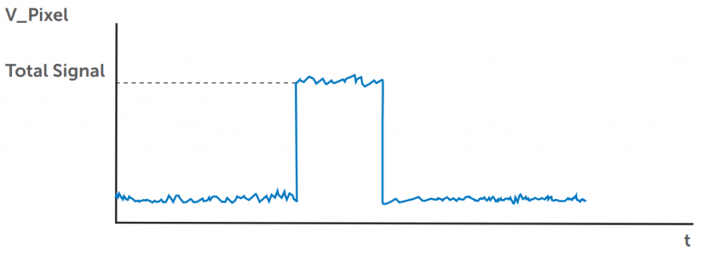
Once the photoelectron charge is converted to a voltage, each pixel holds a peak voltage, indicating how much signal was measured. The longer the exposure, the more voltage builds up in a pixel, and the higher the peak. Once voltages are moved off to ADCs for digitization, the pixel returns to base voltage levels. This is represented in Figure 1.
The first thing to note is that pixel voltage fluctuates, both at the base level and the total recorded signal. These fluctuations are sources of noise for sCMOS cameras, and through the use of correlated sampling, they can be reduced.
The process of reading the total signal off a pixel is subject to read noise, which can affect the signal-to-noise (SNR) ratio of imaging applications, especially those with a low signal level. Two of the main components of read noise are reset noise (also known as kTC noise) and amplifier noise, both of which can be countered with correlated sampling methods.
Reset Noise and Correlated Double Sampling
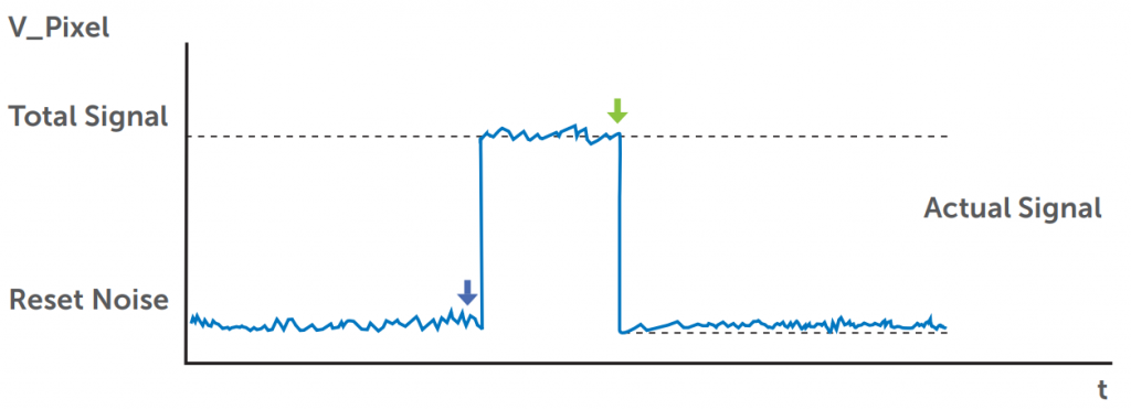
Reset noise is a random offset created when a pixel is cleared of the previous voltage, and can largely be eliminated using a type of sampling known as Correlated Double Sampling (CDS). CDS measures both the base voltage level (reset noise) and the signal voltage level (total signal) in a pixel and subtracts one from the other in order to remove background noise, correct fluctuations, and obtain an accurate measurement free of reset noise, as seen in Fig.2.
By sampling in this manner, CDS can reduce read noise by largely eliminating reset noise, therefore improving camera SNR and sensitivity. However, amplifier noise is still present and is now the dominant source of noise.
Amplifier Noise and Correlated Multi Sampling
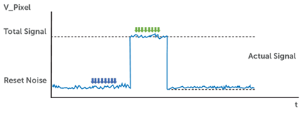
Amplifier noise has a high-frequency white noise component and a low-frequency 1/f component, the latter being particularly difficult to remove. Our solution at Teledyne Photometrics is to sample the base offset level and signal levels multiple times and average the results. This special implementation of CDS is called Correlated Multi-Sampling (CMS) and can be done two or more times, as seen in Fig.3.
Through the use of CMS mode, camera read noise can be reduced to extremely low levels, allowing for highly sensitive imaging. CMS is implemented on the Kinetix family and Prime BSI Family, resulting in low read noises and easy detection of ultra-low signals.

Multi Correlated Multi Sampling and Sub-Electron Read Noise
The above implementation of CMS can also be referred to as 2x CMS, this results in a significant reduction in read noise with a slight cost to speed. However, CMS can sample more than twice, and by implementing 8x CMS or Multi CMS (MCMS) (Fig.4), read noise values fall below one electron to extremely low values, similar to that of an EMCCD with large EM gain values, but without the numerous drawbacks of EMCCD technology. This implementation of 8x CMS in the Kinetix family is known as Sub-Electron mode.
With Sub-Electron mode the most extreme and lowest signal can be imaged, even if a sample only emits a handful of photons! This implementation of MCMS has a larger impact on speed, which should be considered when working with fast-moving dynamic samples.
Signal To Noise Ratio
The effect of CDS and CMS on the SNR using the Signal To Noise equation can further demonstrate their impact on read noise, with other sources of noise (such as photon shot noise) being omitted as they are not affected by correlated sampling methods.
A basic implementation of CDS has a nominal effect on the SNR, as amplifier noise is still present:
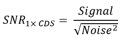
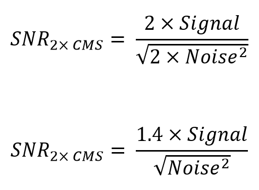
Due to 2x CMS mode sampling twice, there is 2x the signal and only √2x the noise, resulting in a theoretical 1.4x increase in the signal, improving the SNR of the measurement with 2x CMS. The signal level itself is not changing, this SNR increase is mainly due to the reduction of amplifier noise. This makes it possible to achieve read noise levels close to 1 electron with CMS-capable CMOS sensors, allowing for sensitive imaging.
With 8x CMS or MCMS mode, the equation works out to a 2.8x theoretical increase in signal, overall leading to sub-electron read noises of ~0.7 e- for extreme sensitivity.
Using Multiple Signal Chains
Typically, sampling the signal multiple times for CMS comes with a negative impact to frame rate, as each sampling introduces a delay to the readout process. This delay is equal to the time it takes to digitize a pixel. In order to avoid impacting camera speed when using CMS mode, CMS-capable CMOS sensors can use two separate signal chains to simultaneously perform 2x CMS.
Our CMOS sensors use on-chip ADCs that converts the signal voltage to an 11-bit or 12-bit grey level, resulting in a limited dynamic range. This is typically addressed by making two measurements of the voltage in each pixel, the first with very high sensitivity (high-gain) but limited to a max signal of ~1000 electrons, and the second with reduced sensitivity (low-gain) but capable of measuring signals up to the full well capacity of ~45,000 electrons. By combining these two measurements our cameras can make use of a 16-bit mode, thanks to digital gain combining.
This combination of a high-gain and low-gain signal chain allows our CMOS cameras to deliver a large dynamic range and high sensitivity. However, it can also be used to reduce the impact of CMS mode on speed, where the low-gain amplifier can be reconfigured to a second high-gain amplifier, so now two high-gain measurements are being combined. This allows CMS to reduce the read noise in the measurement without a significant trade-off in frame rate. The trade-off instead comes as a reduction in dynamic range due to the limited full-well capacity, as CMS mode typically operates at 11-bit or 12-bit. But it should be noted that as CMS mode is a tool to reduce read noise and increase sensitivity, it is often used at low signal levels that can easily be accommodated by a 12-bit mode.
In this manner, the Kinetix family and Prime BSI family deliver sensitivity with speed, allowing for low read noises across the whole sensor while retaining the characteristic high speeds of CMOS sensors.
Summary
Correlated Multi-Sampling or CMS mode allows our Prime BSI, Prime BSI Express, Kinetix, and Kinetix22 CMOS cameras to maintain a high level of sensitivity when imaging at low light, thanks to the reduction to major components of read noise: reset noise and amplifier noise. This increases the signal-to-noise ratio and showcases how we at Teledyne Photometrics continually work towards high image quality in each of our cameras.