
Introduction
Cameras are incredible tools that allow us to capture and make sense of the visible world around us. Most mobile phones made today come with a camera, meaning that more people than ever are becoming familiar with camera software and taking images. But one of the largest applications of cameras is for scientific imaging, in order to take images for scientific research. For these applications, we need carefully manufactured scientific cameras.
What Is Light?
The most important aspect of a scientific camera is the ability to be quantitative, being a camera that can measure specific quantities of something. In this case, the camera is measuring light, and the most basic measurable unit of light is the photon.
Photons are particles that make up all types of electromagnetic radiation, including light and radio waves, as seen in Figure 1. The most important part of this spectrum for imaging is visible light, which ranges from 380-750 nanometers, as seen in the insert of Figure 1.

As microscopes typically use visible light in the form of a lamp or laser, a scientific camera is essentially a device that needs to detect and count photons from the visible light portion of the spectrum (380‑750 nm), but some applications can also benefit from detection in the UV and IR regions. To do this, scientific cameras use sensors.
Sensors
A sensor for a scientific camera needs to be able to detect and count photons, and then convert them into electrical signals. This involves multiple steps, the first of which involves detecting photons. Scientific cameras use photodetectors, where photons that hit the photodetector are converted into an equivalent amount of electrons. These photodetectors are typically made of a very thin layer of silicon. When photons from a light source hit this layer, they are converted into electrons. A layout of such a sensor can be seen in Figure 2.

Pixels
However, having just one block of silicon means it isn’t clear where the photons come from when they land, it would only be possible to know that they landed. By making a grid of many tiny squares of silicon, photons can be both detected and localized. These tiny squares are referred to as pixels, and technology has developed to the point where you can fit millions of them onto a sensor. When a camera advertises as having 1 megapixel, this means the sensor is an array of one million pixels. This concept is explored in Figure 3.
In order to fit more pixels onto sensors, pixels have become very small, but as there are millions of pixels the sensors are still quite large in comparison. The Prime BSI camera has 6.5 µm square pixels (an area of 42.25 µm2) arranged in an array of 2048 x 2048 pixels (4.2 million pixels), resulting in a sensor size of 13.3 x 13.3 mm (area of 177 mm2 or 1.77 cm2) and a diagonal of 18.8 mm.
Making pixels smaller allows for more to fit on a sensor, but if pixels become too small they won’t be able to detect as many photons, which introduces the concept of compromise in camera design between resolution and sensitivity.
In addition, if sensors are too big or contain too many pixels it would massively increase the computational power needed to process the output information, which would slow down the image acquisition. Large information storage would be needed, and with researchers taking thousands of images in experiments lasting months/years, having a bloated sensor would quickly become an issue as the storage fills up. Due to these reasons the overall sensor size, pixel size and the number of pixels is carefully optimized in camera design.
Generating An Image
When exposed to light, each pixel of the sensor detects how many photons come into contact with it. This gives a map of values, where each pixel has detected a certain number of photons. This array of measurements is known as a bitmap and is the basis of all scientific images taken with cameras, as seen in Figure 4. The bitmap of an image is accompanied by the metadata, which contains all the other information about the image, such as the time it was taken, camera settings, imaging software settings, and microscope hardware information.
The following are the processes involved in generating an image from light using a scientific camera:
- Photons that hit photodetector are converted into electrons (called photoelectrons).
- The rate of this conversion is known as quantum efficiency (QE). With a QE of 50%, only half of the photons will be converted to electrons and information will be lost.
- The generated electrons are stored in a well in each pixel, giving a quantitative count of electrons per pixel
- The maximum number of electrons that can be stored in the well controls the dynamic range of the sensor. This can be described as well depth or bit depth.
- The electron numbers per well are converted from a voltage into a digital signal with an analogue to digital converter (ADC)
- The rate of this conversion is known as gain. With a gain of 1.5, 100 electrons are converted to 150 grey levels. The color generated from 0 electrons is known as the offset.
- These digital signals are known as grey levels and are arbitrary greyscale (monochrome) colors
- What does a grey level of 1 or 100 look like? It depends on the number of electrons in the well and the dynamic range. If there are 100 electrons, 100 grey levels would be bright white. If there are 10,000 electrons, 100 grey levels would be very dark.
- The map of grey levels are displayed on the computer monitor
- The generated image depends on the software settings, such as brightness, contrast, etc.
These steps are visualized in Figure 4.
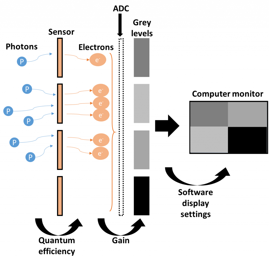
These grey levels vary depending on the number of electrons stored in the sensor pixels. It is also related to two important imaging concepts, offset and gain. Offset is the grey level value from no electrons, the base level. Gain is the conversion factor of electrons to grey levels, for example, 60 electrons can be converted to 60 grey levels (1x gain), or 140 grey levels (2.3x gain). Further relationships between grey levels and the image that appears on the monitor are due to the imaging software display settings. These display settings affect what the grey levels actually look like, as they are otherwise arbitrary (what does 140 grey levels look like, is it the whitest or blackest pixel?) and reliant on the dynamic range of other values across the sensor. These main stages of imaging with a scientific camera are consistent across all modern camera technologies, but there are several different archetypes.
Types Of Camera Sensor
Camera sensors are at the heart of the camera and have been subject to numerous different iterations over the years. Researchers are constantly on the lookout for better sensors which can improve their images, bringing better resolution, sensitivity, field of view and speed. The three main camera sensor technologies are charge-coupled device (CCD), electron-multiplied CCD (EMCCD) and complementary metal-oxide-semiconductor (CMOS), all of which are discussed in separate documents.
Summary
A scientific camera is a vital component of any imaging system. These cameras are designed to quantitatively measure how many photons of light hit which part of the camera sensor. Photons generate electrons (photoelectrons), which are stored in sensor pixels and converted to a digital signal, which is displayed as an image. This process is optimized at every stage in order to produce the best possible image depending on the signal received. Read on for more about the three main types of sensor, the CCD, EMCCD and CMOS.