
Introduction
CCDs are well-established scientific sensors for cameras. A major benefit of CCD sensors is the extremely low dark current that allows long exposure imaging. In contrast, CMOS sensors have dark currents 100-1000x greater than CCDs. But what if CMOS camera sensors were also capable of long exposure imaging, thanks to new thermal control technologies? When compared to CCDs, CMOS sensors typically have greater speeds, larger sensor sizes, and continual improvements with long-term support.
This technical note introduces the Retiga E7 CMOS, and how optimized thermal control provides a low dark current that can open up a whole new world of imaging with CMOS.
What Is Dark Current?
Light and heat both create signals in sensors. As a camera sensor is exposing, both photons from the light source and heat from the electronics or environment cause charge to build up in the pixel. Unfortunately, the charge from heat can’t be differentiated from the photoelectrons generated on the camera sensor from light. As the sensor cannot determine between thermal electrons or photoelectrons, heat contributes a background signal that can’t be separated from the signal from light. The mathematical properties of photon signal and heat signal are identical. Just as light intensity has shot noise, thermal signal has dark current noise. The averages of the dark current can be subtracted from the image, but the dark current noise still remains.
Dark current is typically measured in electrons per pixel per second (e–/p/s). The last metric is the most important, the lower the exposure time, the lower the dark current. With highly sensitive and fast scientific CMOS cameras, long exposure times aren’t as necessary as exposure times are often less than 100 milliseconds. These short exposures result in negligible dark current build-up. But if an experiment requires long exposure times (seconds to minutes), the dark current of current CMOS cameras becomes a significant contributor to background and noise.
Because the dark current is a thermal effect independent of the light level it can be reduced with cooling. For 6-7 °C of cooling of the camera sensor, the effects of dark current are approximately halved. This is why scientific cameras are often cooled. Lower operating temperatures reduce the dark current and result in a higher signal-to-noise ratio, key to getting high-quality results.
CCDs for Long Exposure Imaging
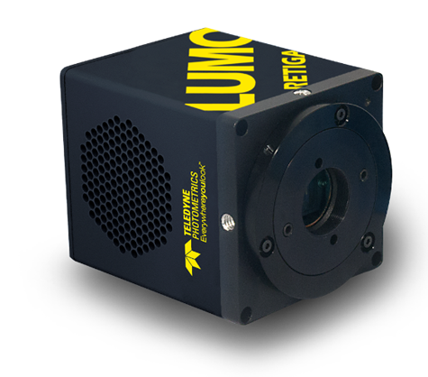
CCDs naturally have an extremely low dark current, making them suitable for experiments that require long exposure times. This is taken to the extreme with Teledyne Photometrics’ Retiga LUMO CCD, which is optimized for exposures of over an hour, suitable for imaging luminescence.
However, CCD technology comes with a number of disadvantages, such as high read noise, low maximum speed, clock timing complications, and smaller sensor size. The smaller full well capacity of CCD sensor pixels can also lead to saturation, blooming, and streaking when dealing with intense signals or long exposures.
Many areas of quantitative research in the life sciences have adopted CMOS camera technologies, which feature higher speeds, larger FOVs, and lower read noise.
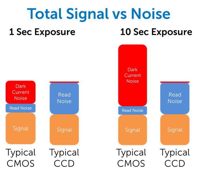
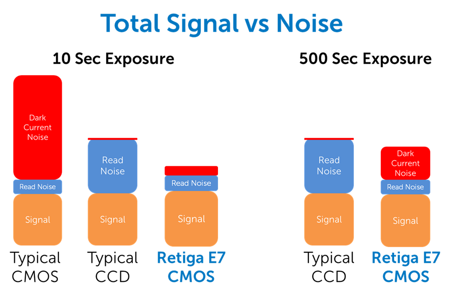
But the advantages of CMOS technology all come at the cost of significantly higher dark current. While the Retiga LUMO CCD has a dark current of 0.0001 e–/p/s, the Prime 95B CMOS has a dark current of 0.55 e–/p/s (with air cooling). The read noise of the CMOS is significantly lower compared to the CCD (1.6 e– compared to 4.5 e–), but the dark current is several magnitudes greater and leads to significant dark current noise build-up when imaging at exposures beyond 2-3 seconds. This makes for different total noise contributions for CCD vs CMOS at longer exposures, as shown in Fig.2.
What is needed is a CMOS sensor with advanced thermal control, this will reduce the dark current and allow for long exposure imaging with a CMOS, with all the additional advantages this will bring.
The Retiga E7 CMOS
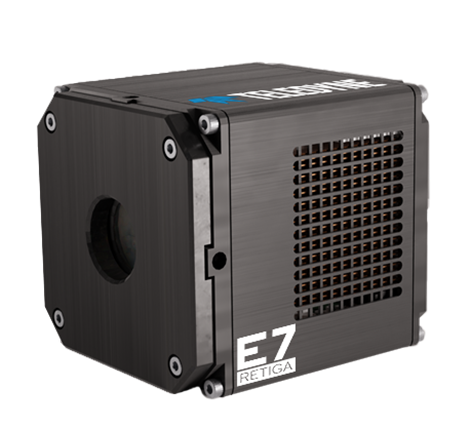
The all-new Retiga E7 CMOS is just such a camera, featuring an ultra-low dark current of 0.02 e–/p/s, allowing for high signal-to-noise ratio imaging at long exposures, up to 20 minutes and beyond!
There are three main areas where the Retiga E7 excels in thermal control and the resulting image quality at long exposures: mechanical, electrical, and firmware. Combining our industry-leading expertise in these areas has resulted in a CMOS that competes with CCDs for long exposure imaging.
Mechanical Heat Handling
As explained further in our Citadel Chamber Design tech note, the mechanical design of the camera internal components is vital for the effective and even cooling of the camera sensor. Uneven sensor cooling leads to hotspots and image artifacts. Many factors contribute to the uniform sensor cooling and chamber stability found in Teledyne Photometrics cameras.
Our Citadel chamber technology is a result of 40 years of experience designing and implementing sensor cooling. A Mean Time Before Failure (MTBF) of greater than 10 years demonstrates the result of our experience. This experience has been applied to optimizing thermal controls within the Retiga E7. The resulting uniform low sensor temperature and the resultant low dark current brings long exposure imaging to scientific CMOS cameras.

Electronics
The ‘Readout’ electronics on CMOS sensors are a major source of heat during exposure, meaning the electronic design of the sensor has a big impact on the eventual dark current.
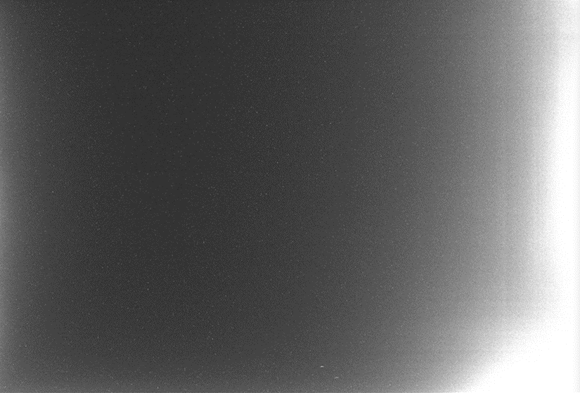
Our aim with the Retiga E7 CMOS was to minimize the amount of heat generated by the camera electronics and reduce the creation of thermal noise during the crucial phase of exposure. The position of the Readout electronics along the edge of CMOS sensors often leads to the build-up of heat along the edge of the sensor and a visible ‘glow’ at certain edges. This glow can then spread towards the center of the sensor as exposure times get longer and longer. By minimizing the heat generation in the electronic systems at these edge hotspots, the overall thermal generation can be reduced. An example of heat generation at the sensor edge can be seen in Fig.5.
In addition, there are external sources of electronic noise. With poorly designed scientific cameras, electronic noise from the camera power supply can reach the sensor, adding significant uncertainty to measurements and reducing image quality. There exists a relationship between power supply voltage fluctuations/ripples and potential sensor noise, but Teledyne Photometrics has eliminated this issue in CMOS thanks to our extensive experience in this area.
Firmware
Between the careful mechanical design and highly optimized electronic design, the majority of thermal generation and dark current can be addressed. To optimize for long exposures even further, we also implement firmware solutions.
At Teledyne Photometrics we make measurements on each camera in order to understand that individual camera’s thermal characteristics. By characterizing their thermal behavior, we can then store calibration data on the camera. This leads to reduced noise and a flat, clean bias critical to the quality of every image taken with the camera.
Even if the thermal design is done well, heat gradients still exist due to the edge positioning of the CMOS readout electronics. This is corrected for each camera using ‘Dynamic Dark Frame Correction’ technology, based on the measured thermal accumulation at the site of readout.
Another firmware solution is ‘despeckling’, which corrects pixel-to-pixel thermal variations based on the individual calibration data. These ‘hot pixels’ decrease the overall image quality and can make for significant artifacts, at Teledyne Photometrics we correct these hotspots without impacting the image quality.
This combination of different firmware calibrations leads to striking improvements in image quality when compared to raw images, as seen from the comparison of Fig.6 vs the raw image from Fig.5.

In addition, there are external sources of electronic noise. With poorly designed scientific cameras, electronic noise from the camera power supply can reach the sensor, adding significant uncertainty to measurements and reducing image quality. There exists a relationship between power supply voltage fluctuations/ripples and potential sensor noise, but Teledyne Photometrics has eliminated this issue in CMOS thanks to our extensive experience in this area.
Summary
The end result is that the total noise contribution for the Retiga E7 CMOS is very low. The combination of low read noise inherent in CMOS sensor architecture and low dark current – from our optimization mechanical, electronic, and firmware – result in low overall total noise. The Retiga E7 is the first CMOS capable of long exposures comparable to those seen using CCDs, but with the large FOV and speeds inherent to CMOS cameras.
All the benefits of CMOS, with a dramatically lower dark current. The Retiga E7 is ideal for long exposure experiments as well as more challenging documentation cases where flexibility is needed.